







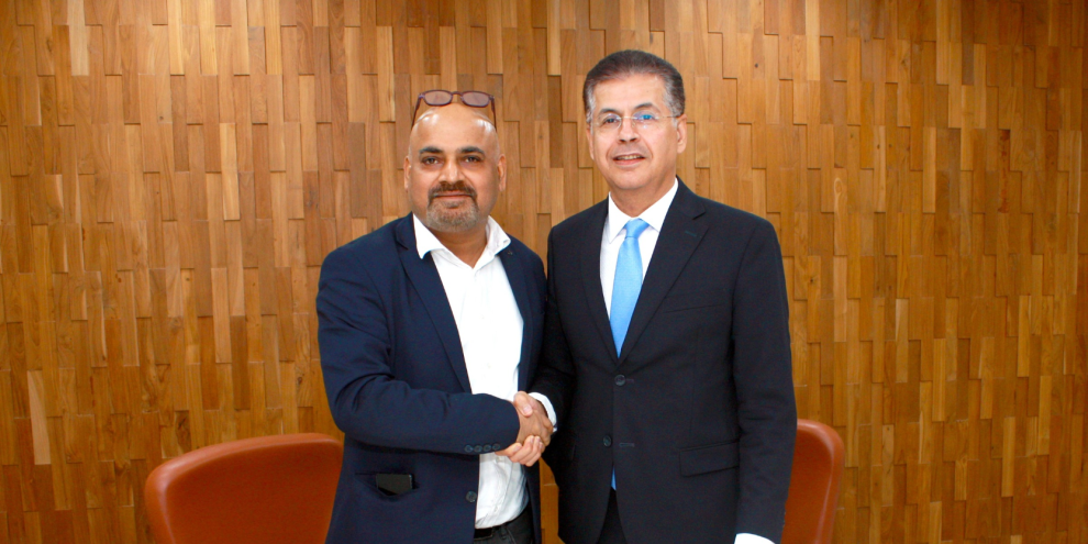
Paras Semiconductors has announced a technology partnership with BroadPak Corporation to develop advanced semiconductor packaging capabilities in India. The collaboration includes plans for an outsourced semiconductor assembly and test facility, technology transfer, chiplet integration and training for Indian engineers.
The Paras Defence subsidiary will work with US based BroadPak Corporation to develop a proposed semiconductor assembly and testing facility supporting 2.5D and 3D integration, chiplet technologies, AI and high performance computing applications.
Advanced Chip Packaging in India Gets a Push as Paras Semiconductors Partners with BroadPak
Mumbai, November 6, 2026: Paras Semiconductors, a subsidiary of Paras Defence & Space Technologies Limited, has entered into a strategic technology partnership with US based BroadPak Corporation to develop advanced semiconductor packaging capabilities in India.
The collaboration aims to establish an advanced heterogeneous integration and 3D packaging facility operating under the outsourced semiconductor assembly and test (OSAT) model.
The proposed facility will focus on technologies including 2.5D and 3D semiconductor packaging, chiplet integration, hybrid bonding, wafer level and panel level fan out packaging, co packaged optics and semiconductor testing.
The agreement brings together Paras Semiconductors’ plans to expand into semiconductor manufacturing and BroadPak’s expertise in advanced packaging design, integration and production processes.
BroadPak Corporation, headquartered in San Jose, California, was established in 2007. Its work covers heterogeneous integration, multidie architectures, high speed interconnects, thermal management and semiconductor packaging.
The company provides capabilities across architecture development, design, simulation, assembly, testing and production.
Under the partnership, Paras Semiconductors will gain access to BroadPak’s design, manufacturing and integration intellectual property, along with technology transfer and process knowledge related to advanced packaging and chiplet integration.
The companies also intend to explore the joint development of packaging platforms for artificial intelligence and high performance computing applications.
Training and skill development for Indian engineers will form another part of the collaboration.
The proposed OSAT facility is intended to support high volume manufacturing requirements across strategic electronics, optical and optronic systems, networking, data centres and computing applications.
Its planned technical capabilities include wafer level processing, hybrid bonding, through silicon vias, micro bumping, advanced interposers, redistribution layer technologies, co packaged optics and reliability testing.
These processes are used to connect and integrate semiconductor components within advanced packages, particularly where multiple processing and memory elements must operate together.
Munjal Sharad Shah, Managing Director, Paras Defence & Space Technologies Limited, described the partnership as an expansion of the company’s technology activities.
He said, “Our entry into the semiconductor sector represents a strategic expansion into a technology domain that is increasingly critical to India’s AI and data centres and industrial capabilities. With Paras Semiconductors, we are looking to build capabilities in advanced packaging that complement our existing strengths in optics, optronics and critical electronics. Our collaboration with BroadPak brings the specialised technology expertise required to accelerate this ambition and develop capabilities that can serve both strategic domestic requirements and the wider semiconductor industry.”
Santosh Kumar, Chief Executive Officer, Paras Semiconductors, discussed the technical requirements driving the company’s plans.
He said, “The semiconductor industry’s requirements are evolving beyond conventional chip manufacturing towards advanced integration of multiple dies, memory and processing components within a single package. Our collaboration with BroadPak will help us develop capabilities across 2.5D/3D heterogeneous integration, chiplet architectures, hybrid bonding and advanced system-in-package technologies. We intend to build an advanced packaging platform that can address the increasingly complex performance, connectivity and thermal requirements of next-generation semiconductor applications.”
Dr. Farhang Yazdani, Founder and Chief Executive Officer, BroadPak Corporation, said the collaboration would bring the company’s semiconductor packaging expertise to India.
He said, “Advanced packaging is becoming central to the next generation of semiconductor innovation, particularly as AI and high-performance computing push the boundaries of conventional chip architectures. India’s growing semiconductor ecosystem presents an important opportunity to develop capabilities in heterogeneous integration and system-level packaging. Through our collaboration with Paras Semiconductors, we look forward to bringing our expertise in advanced packaging technologies, engineering and manufacturing processes to support the development of these capabilities in India.”
Dr. Yazdani has more than two decades of semiconductor industry experience and is the inventor of 3DHI HiRise Packaging Technology. His work includes heterogeneous integration, chiplet architectures, silicon photonics and co packaged optics.
The partnership comes as semiconductor manufacturers increasingly examine advanced packaging methods for AI accelerators, graphics processing units, high bandwidth memory and other computing systems.
According to Yole Group estimates presented at the 2026 IMAPS Device Packaging Conference, the global advanced packaging market is projected to increase from more than US$40 billion in 2024 to over US$80 billion by 2030.
The press announcement also refers to NITI Aayog’s 2026 semiconductor industry roadmap, which identifies 2.5D and 3D integration, chiplet assembly, fan out packaging and system in package technologies as priority areas for domestic manufacturing development.
For Paras Defence, the proposed initiative represents an extension of its existing activities in optics, optronics, defence electronics and other critical technologies.
Paras Defence & Space Technologies Limited operates across Optics & Optronic Systems and Defence Engineering, including defence electronics, electromagnetic pulse protection and heavy engineering.
BroadPak’s experience in semiconductor packaging and system integration is expected to support the proposed development of domestic assembly, testing and advanced integration capabilities.
The companies have outlined plans for technology transfer, engineering training and packaging platform development. The announcement does not specify the facility’s location, investment value, production capacity or commissioning schedule.
At Prittle Prattle News, featuring you virtuously, we celebrate the commitment and innovation. Led by Editor-in-Chief Smruti Bhalerao, our platform is dedicated to sharing impactful stories that inspire change and create awareness. Follow us on LinkedIn, Instagram, and YouTube for more stories that matter.
About Prittle Prattle News
Prittle Prattle News is a digital news publication covering business, technology, healthcare, education, lifestyle, public affairs and other developments from India and around the world. Led by Editor-in-Chief Smruti Bhalerao, we publish timely news, industry updates and feature stories for a broad readership.




















Add Comment