The Mumbai-based institute’s work, built under the Chips to Startup programme and fabricated at SCL Mohali, became part of India’s semiconductor showcase in Bengaluru attended by Prime Minister Narendra Modi
Student engineers from Vivekanand Education Society’s Institute of Technology (VESIT) have entered uncharted territory for a private college in Maharashtra. Their indigenously designed integrated circuit was among the projects featured at Semicon India 2025, the country’s flagship platform for semiconductor self-reliance.
The chip, a Programmable Gate Array Integrated Circuit (PGA IC), was developed under the Government of India’s Chips to Startup (C2S) programme and fabricated at the Semiconductor Laboratory (SCL), Mohali, using 180 nm CMOS technology. It is one of the first designs from a private autonomous institute in the state to move from classroom research into national-level demonstration.
Faculty members at VESIT said the project was carried out by a student team working under the mentorship of the electronics department. The design, they explained, is aimed at bridging the gap between theoretical learning and practical semiconductor development, a gap that is often only filled at IITs or public research institutions.
The Bengaluru event, inaugurated by Prime Minister Narendra Modi, highlighted India’s ambition to grow its domestic chip ecosystem and reduce import dependence. For VESIT, inclusion in the showcase marks recognition that private colleges can contribute directly to this mission.
The institute, affiliated with the University of Mumbai but operating as an autonomous entity, described the opportunity as proof of what student-led innovation can achieve when supported by national programmes like C2S.
Observers in the semiconductor community said the appearance of VESIT at Semicon India signals a widening of the base of talent contributing to chip design in India a field where the country has strength in design talent but limited fabrication success.
As the global race for semiconductor independence intensifies, the recognition of a student-built chip from Mumbai is being seen as both symbolic and practical: symbolic because it widens India’s innovation base, practical because it encourages more private institutes to enter the domain.
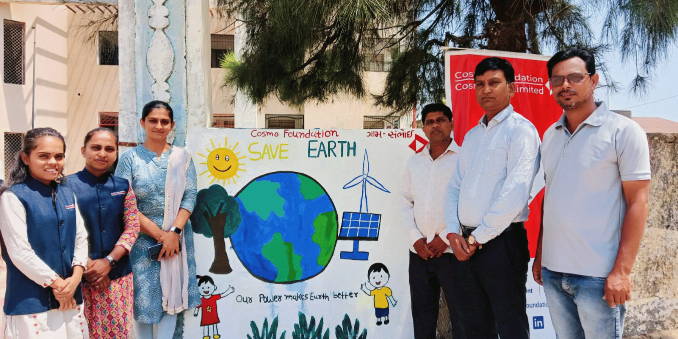
At Prittle Prattle News, we honor your dedication and inventiveness led by showcasing you in a positive light. Under the direction of Editor-in-Chief Smruti Bhalerao, our platform is committed to disseminating powerful narratives that raise awareness and motivate change. For more important stories, follow us on LinkedIn, Instagram, and YouTube.


naturally like your web site however you need to take a look at the spelling on several of your posts. A number of them are rife with spelling problems and I find it very bothersome to tell the truth on the other hand I will surely come again again.
I truly appreciate your technique of writing a blog. I added it to my bookmark site list and will
I really like reading through a post that can make men and women think. Also, thank you for allowing me to comment!
https://shovelhunter.com/
https://shovelhunter.com/
https://shovelhunter.com/
This was beautiful Admin. Thank you for your reflections.
탑플레이어포커머니상
I do not even understand how I ended up here, but I assumed this publish used to be great
https://shovelhunter.com/
https://galindoslowriderbikes.com/product/toplowrider/
https://shovelhunter.com/
https://galindoslowriderbikes.com/product/toplowrider/
https://galindoslowriderbikes.com/product/toplowrider/
Hi there to all, for the reason that I am genuinely keen of reading this website’s post to be updated on a regular basis. It carries pleasant stuff.
Great information shared.. really enjoyed reading this post thank you author for sharing this post .. appreciated
For the reason that the admin of this site is working, no uncertainty very quickly it will be renowned, due to its quality contents.
I very delighted to find this internet site on bing, just what I was searching for as well saved to fav
I really like reading through a post that can make men and women think. Also, thank you for allowing me to comment!
I do not even understand how I ended up here, but I assumed this publish used to be great
Awesome! Its genuinely remarkable post, I have got much clear idea regarding from this post
This is my first time pay a quick visit at here and i am really happy to read everthing at one place
Awesome! Its genuinely remarkable post, I have got much clear idea regarding from this post
I appreciate you sharing this blog post. Thanks Again. Cool.
[…] being a legacy auto components company to one of India’s most influential names in sustainable mobility. With over 300,000 Ampere scooters sold to date and a growing nationwide charging and service […]
流媒体成人内容 通过选择经过验证的成人网站来安全进行。使用 有保障的来源
以获得私密的娱乐体验。
My web site: buy xanax without prescrition